Constructing, Designing, and Testing the Forward Bias of a PN Junction Using AutoCAD
Experiment Name:
Constructing, Designing, and Testing the Forward Bias of a PN Junction Using AutoCAD
Theory:
A PN junction is a fundamental building block of semiconductor devices. It is formed by joining P-type and N-type semiconductors together in very close contact. The P-type semiconductor contains an excess of holes (positive charge carriers), while the N-type contains an excess of electrons (negative charge carriers).
When a forward bias is applied to a PN junction (the P-side is connected to the positive terminal of a power supply and the N-side to the negative terminal), the potential barrier at the junction decreases, allowing current to flow through the device. This behavior is crucial for the operation of diodes, transistors, and other semiconductor devices.
The forward bias condition reduces the width of the depletion region, allowing charge carriers to recombine across the junction and facilitating current flow. This experiment aims to design and test the forward bias of a PN junction using AutoCAD for the design and simulation part.
Apparatus:
Computer with AutoCAD software installed
PN junction design schematic
Power supply (for practical testing, if applicable)
Multimeter (for measuring voltage and current)
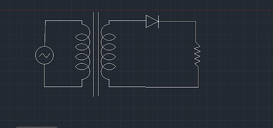
Circuit Diagram:
Procedure:
Design Using AutoCAD:
Open AutoCAD: Start the AutoCAD software on your computer.
Create a New Project: Select "New" to create a new drawing project.
Design the PN Junction:
Draw the P-type and N-type regions using the rectangle tool.
Indicate the depletion region at the interface.
Label the P-type side with "P" and the N-type side with "N".
Circuit Design:
Draw the connections for applying forward bias. This includes drawing the power supply connections.
Use lines to represent the connecting wires.
Insert symbols for the battery (power supply) and the diode (representing the PN junction).
Annotate the Diagram: Add annotations to label the components and connections clearly.
Testing Forward Bias:
Apply Forward Bias:
Connect the positive terminal of the power supply to the P-side of the diode.
Connect the negative terminal of the power supply to the N-side of the diode.
Measure Voltage and Current:
Use a multimeter to measure the voltage drop across the diode.
Measure the current flowing through the circuit.
Simulation (If using AutoCAD for simulation):
Run the Simulation: Use AutoCAD’s simulation tools to analyze the forward bias behavior.
Observe the Results: Note the voltage drop and current flow in the simulation.
Results:
Design Diagram: Include a screenshot or printout of the PN junction design created in AutoCAD.
Voltage Measurement: Record the forward voltage drop observed across the PN junction.
Current Measurement: Record the current flowing through the PN junction under forward bias.
Simulation Output: Provide screenshots or data from the AutoCAD simulation showing the behavior of the PN junction under forward bias.
Discussion:
Design Considerations: Discuss the key aspects of the PN junction design in AutoCAD, such as the dimensions of the P and N regions and the depiction of the depletion region.
Forward Bias Behavior: Explain the behavior observed when the PN junction is forward biased, including the reduction of the depletion region and the facilitation of current flow.
Comparison with Theory: Compare the experimental and simulation results with theoretical expectations. Discuss any discrepancies and possible reasons for them.
Practical Implications: Highlight the significance of understanding the forward bias of PN junctions in practical applications, such as in diodes and transistors.
Limitations and Improvements: Identify any limitations of the experiment or design process and suggest possible improvements for future studies.


মন্তব্যসমূহ
একটি মন্তব্য পোস্ট করুন