পোস্টগুলি

মে, ২০২৪ থেকে পোস্টগুলি দেখানো হচ্ছে

Study of Frequency Shift Keying (FSK)

ছবি
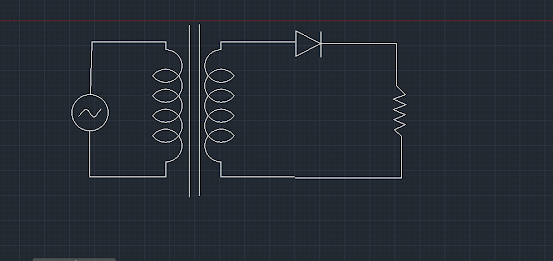
 Experiment Name:  Study of Frequency Shift Keying (FSK) Theory Frequency Shift Keying (FSK) is a digital modulation technique in which the frequency of the carrier signal is varied in accordance with the digital signal data. In FSK, binary data is transmitted through discrete frequency changes of the carrier wave. The most common types of FSK are Binary FSK (BFSK), where two frequencies represent binary '0' and '1', and Multiple FSK (MFSK), where multiple frequencies are used to represent more than two levels of digital data. Circuit Diagram: Apparatus: Function Generator Frequency Counter Oscilloscope Breadboard Connecting Wires Resistors and Capacitors (as required) FSK Modulator IC Power Supply Procedure: Modulation Assemble the FSK modulator circuit on the breadboard according to the provided circuit diagram. Connect the power supply to the circuit. Ensure correct voltage levels as specified for the FSK modulator IC. Connect a binary data signal to the input of the...

Design, Construction, and Testing of a Full-Wave Rectifier using AutoCAD.

ছবি
 Experiment Name: Design, Construction, and Testing of a Full-Wave Rectifier using AutoCAD. Theory A full-wave rectifier is an electronic device that converts an alternating current (AC) input into a direct current (DC) output. Unlike a half-wave rectifier, which uses only one half of the AC waveform, a full-wave rectifier utilizes both halves, thereby increasing the efficiency of the rectification process. A full-wave rectifier typically consists of a transformer, four diodes arranged in a bridge configuration, and a load resistor. The transformer adjusts the input AC voltage to the desired level. The diodes then rectify the AC signal, allowing current to pass through only during specific portions of the AC cycle, effectively flipping the negative halves of the waveform to positive. The result is a pulsating DC voltage that is further smoothed by a capacitor filter to reduce ripples. Apparatus: Transformer (Step-down, Center-tapped) Four diodes (1N4007) Load resistor (1 kΩ) Capaci...

Design, Construction, and Testing of a Half-Wave Rectifier Using AutoCAD

ছবি
 Experiment Name: Design, Construction, and Testing of a Half-Wave Rectifier Using AutoCAD Theory: A half-wave rectifier is an electronic circuit used to convert alternating current (AC) into direct current (DC). It allows only one half of the AC cycle (positive or negative) to pass through, effectively blocking the other half. This process is accomplished using a single diode, which permits current to flow only during one half-cycle of the AC input. In a half-wave rectifier: During the positive half-cycle of the AC input, the diode is forward-biased and conducts, allowing current to pass through to the load. During the negative half-cycle, the diode is reverse-biased and does not conduct, preventing current from reaching the load. The result is a pulsating DC output that contains gaps corresponding to the blocked half-cycles of the AC input. A capacitor is often used to smooth the output, reducing the ripple and providing a more constant DC voltage. Circuit Diagram: Apparatus: Tra...

Study of pulse amplitude modulation

ছবি
Experiment No: Experiment Name: Study of pulse amplitude modulation AIM: To study sampling and reconstruction of Pulse Amplitude modulation system. APP ARATUS REQUIRED:   1. PAM modulator 2.Oscilloscope. 3. Patch cords 2mm  4. Power supply  THEORY:   Pulse Amplitude Modulation - In Pulse Amplitude Modulation message information is encoded in the amplitude of a series of signal pulses. It is an analog pulse modulation scheme in which the amplitude of train of carrier pulse are varied according to the sample value of the message signal. A train of very short pulses of constant amplitude and fast repetition rate is chosen the amplitude of these pulse is made to vary in accordance with that of a slower modulating signal the result is that of multiplying the train by the modulating signal the envelope of the pulse height corresponds to the modulating wave .the Pam wave contain upper and lower side band frequencies besides the modulating and pulse signals. The de...

Design, Construction, and Testing of a Full Adder Circuit Using AutoCAD

ছবি
  Experiment No: Experiment Name:   Design, Construction, and Testing of a Full Adder Circuit Using AutoCAD Theory: A full adder is a digital circuit that performs the addition of three binary bits, producing a sum and a carry value. Unlike the half adder, a full adder includes an additional input to accommodate the carry-in from a previous addition stage, making it a fundamental component in multi-bit binary addition. The full adder operates according to the following truth table Input A Input B Carry-In (Cin)      Sum (S) Carry-Out (Cout)      0              0                 0                 0                0      0              0          1               ...

Design, Construct, and Test of a Half Adder Circuit Using AutoCAD

ছবি
Experiment No: Experiment Name: Design, Construct, and Test of a Half Adder Circuit Using AutoCAD Theory: A half adder is a digital circuit that performs the addition of two binary digits. It has two inputs, usually denoted as A and B, and two outputs: the sum (S) and the carry (C). The half adder's truth table is as follows: A B Sum (S) Carry (C) 0 0         0          0 0 1         1          0 1 0         1          0 1 1            0              1 The Boolean equations for the outputs are: Sum (S) = A XOR B Carry (C) = A AND B These logic gates are fundamental components in digital electronics and are used in more complex arithmetic circuits. Apparatus: Computer with AutoCAD software AutoCAD Electrical toolkit (if available) Digital Logic simulation sof...

Frequency Modulation

ছবি
  Frequency Modulation   Experiment No:   Experiment Name:   Study of Frequency Modulation   Objective: To study and understand the process of frequency modulation by observing the changes in the carrier wave’s frequency in accordance with the message signal’s variations.   Theory: Frequency Modulation (FM) is a method of encoding information on a carrier wave by varying the instantaneous frequency of the wave. In FM, the frequency deviation of the carrier wave is proportional to the amplitude of the input signal (message signal). This technique is widely used in radio broadcasting, telemetry, and other forms of data communication because of its resilience to signal degradation and noise. s(t) = Ac cos(2πfct + 2πkf ∫ T 0   m(τ)dτ where, Ac  is the Amplitude of the Carrier Signal fc  is the Frequency of the Carrier Signal kf  is the Frequency Deviation Sensitivity m(t)  is the Modulating...

Amplitude Modulation

ছবি
  Amplitude Modulation   Experiment No: Experiment Name: Study of Amplitude Modulation   Objective: To study and understand the process of amplitude modulation by observing the changes in the carrier wave’s amplitude in accordance with the message signal’s variations.   Theory: Amplitude Modulation (AM) is a technique used in electronic communication, most commonly for transmitting information via a radio carrier wave. In AM, the amplitude (signal strength) of the carrier wave is varied in proportion to that of the message signal being transmitted. This contrasts with frequency modulation (FM) and phase modulation (PM). AM involves modulating a high-frequency carrier signal with a lower-frequency message signal. The modulated signal’s envelope changes proportionally to the voltage of the message signal. The AM signal can be expressed mathematically as: s(t)=(1+m ⋅ cos(2πf m ​t)) ⋅ cos(2πf c ​t) where: (s(t)) is the modulated signal. (m) is...

Design, Construction, and Verification of Basic Logic Gates (AND, OR, and NOT) Using AutoCAD

  Experiment Name Design, Construction, and Verification of Basic Logic Gates (AND, OR, and NOT) Using AutoCAD Theory NOT Gate (Inverter): The NOT gate produces the complement of its input signal. It has one input and one output. When the input is high (1), the output is low (0), and vice versa. The truth table for a NOT gate: Table Input (A) Output (Y) 0 1 1 0 AND Gate: The AND gate produces a high output only when both inputs are high. It has two inputs and one output. The truth table for an AND gate: Table Input A Input B Output Y 0 0 0 0 1 0 1 0 0 1 1 1 OR Gate: The OR gate produces a high output if any input is high. It also has two inputs and one output. The truth table for an OR gate: Table Input A Input B Output Y 0 0 0 0 1 1 1 0 1 1 1 1 Apparatus AutoCAD software Computer with appropriate system requirements Circuit components (resistors, wires, etc.) Procedure NOT Gate (Inverter): Create a schematic diagram for the NOT gate using AutoCAD. Label the input and output termin...