Design, Construction, and Testing of a Full Adder Circuit Using AutoCAD
Experiment No:
Experiment Name: Design, Construction, and Testing of a Full Adder Circuit Using AutoCAD
Theory:
A full adder is a digital circuit that performs the addition of three binary bits, producing a sum and a carry value. Unlike the half adder, a full adder includes an additional input to accommodate the carry-in from a previous addition stage, making it a fundamental component in multi-bit binary addition.
The full adder operates according to the following truth table
Input A Input B Carry-In (Cin) Sum (S) Carry-Out (Cout)
0 0 0 0 0
0 0 1 1 0
0 1 0 1 0
0 1 1 0 1
1 0 0 1 0
1 0 1 0 1
1 1 0 0 1
1 1 1 1 1
Boolean Expressions
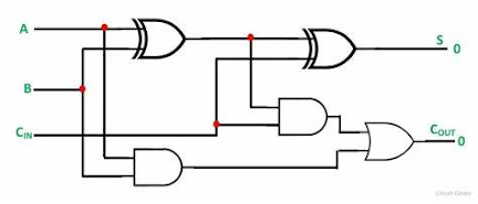
Sum (S) = A ⊕ B ⊕ Cin (XOR gates)
Carry-Out (Cout) = (A · B) + (B · Cin) + (Cin · A) (AND and OR gates)
Apparatus
AutoCAD software for designing the circuit
Components for simulation (if using an AutoCAD plugin like AutoCAD Electrical)
Computer system with adequate specifications to run AutoCAD.
Circuit Diagram:
Procedure:
Design the Circuit Using AutoCAD:
Open AutoCAD and create a new drawing.
Use appropriate symbols to represent the full adder components (XOR gates, AND gates, and OR gate).
Connect the inputs (A, B, and CARRY IN) to the gates and obtain the SUM and CARRY OUT outputs.
Save the design.
Construct the Circuit
If you’re building a physical circuit, gather the required components (breadboard, gates, wires).
Connect the gates according to the AutoCAD design.
Ensure proper connections between inputs and outputs.
Power the circuit using a suitable power supply.
Test the Full Adder Circuit:
Apply binary inputs (0 or 1) to A, B, and CARRY IN.
Observe the SUM and CARRY OUT outputs.
Verify that the SUM output matches the expected result.
Check if the CARRY OUT indicates any carry during addition.
Discussion
The full adder circuit successfully combines two half adders to perform addition with carry-in. AutoCAD facilitates the design process, allowing precise placement of components. Testing ensures that the circuit operates as expected.

মন্তব্যসমূহ
একটি মন্তব্য পোস্ট করুন